| Definition: | central area of a wafer surface, defined by a nominal edge exclusion, X, over which the specified values of a parameter apply
Note 1 to entry: The nominal edge exclusion, X, is usually 5 mm as shown in Figure 1.
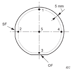
Figure 1 – Wafer sketch and measurement points
|